
Vertex Systems Oy does not have its own PCB design software.
For design work, Vertex ED focuses on electrical design (Vertex ED and HD product documentation), but it does not include PCB design.
Printed circuit board – Wikipedia
This article outlines the basic steps of PCB design using the free KiCad software through a hobby project, and importing the finished PCB’s 3D model into Vertex G4 for further processing.
You can download KiCad here: KiCad EDA – Schematic Capture & PCB Design Software
There are many tutorial videos for learning the software, for example on YouTube:
(1787) kicad tutorial for beginners – YouTube
Main steps in PCB design
1. Concept design
-
Sketch the circuit diagram on paper for the PCB you want to design
-
Or copy an existing schematic
-
Adjust as needed based on project requirements
2. Circuit design in KiCad
-
Open the Schematic Capture section in KiCad: Schematic Capture in Eeschema | KiCad EDA
-
Create the schematic using the built-in symbol library or import symbols from online libraries (KiCad already includes a comprehensive library)
-
Draw connections between components
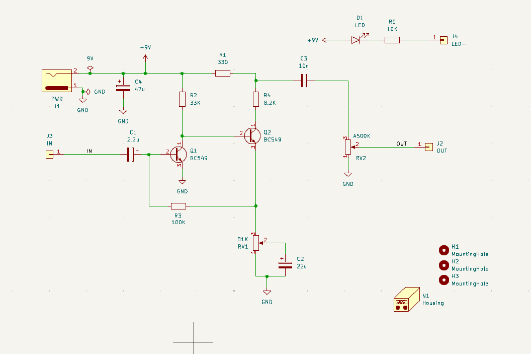
Example:
A simple schematic of a guitar fuzz pedal with two transistors and two potentiometers (volume and distortion level), powered by 9 V.
This is a variation of the 1960s Fuzz Face pedal.
The PCB in this example is designed for through-hole components for easy soldering with a soldering iron.
KiCad also supports surface-mount components, allowing design of mass-produced PCBs.
Multi-layer boards up to 4 layers are supported.
3. PCB layout in KiCad
-
Once the schematic is complete and tested within KiCad, switch to the PCB layout section: PCB Design in PcbNew | KiCad EDA
-
Because the schematic is made using KiCad symbols, it stays synchronized with the PCB layout
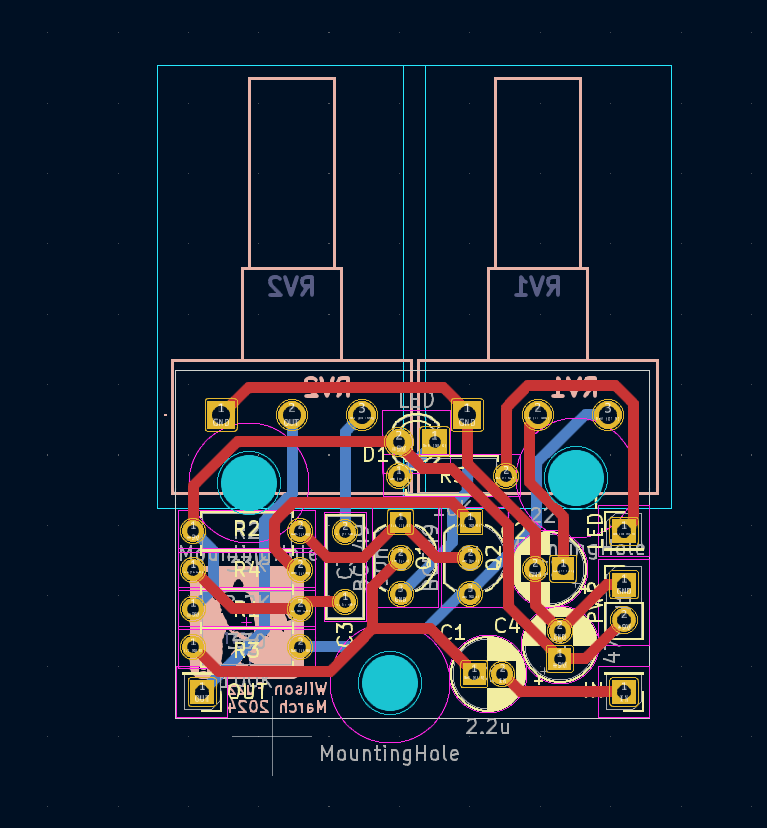
Example finished PCB layout:
-
Mounting holes for components
-
Traces between components
-
Silk screen text printed on the board surface
-
PCB width, length, and mounting pads already defined
4. Preparing files for PCB manufacturing
-
Export schematic, PCB layout, and drill files for the manufacturer
-
Many PCB prototyping services are available online, producing even very small batches
Example: PCBWAY – China PCB Prototype & Fabrication Manufacturer – PCB Prototype the Easy Way
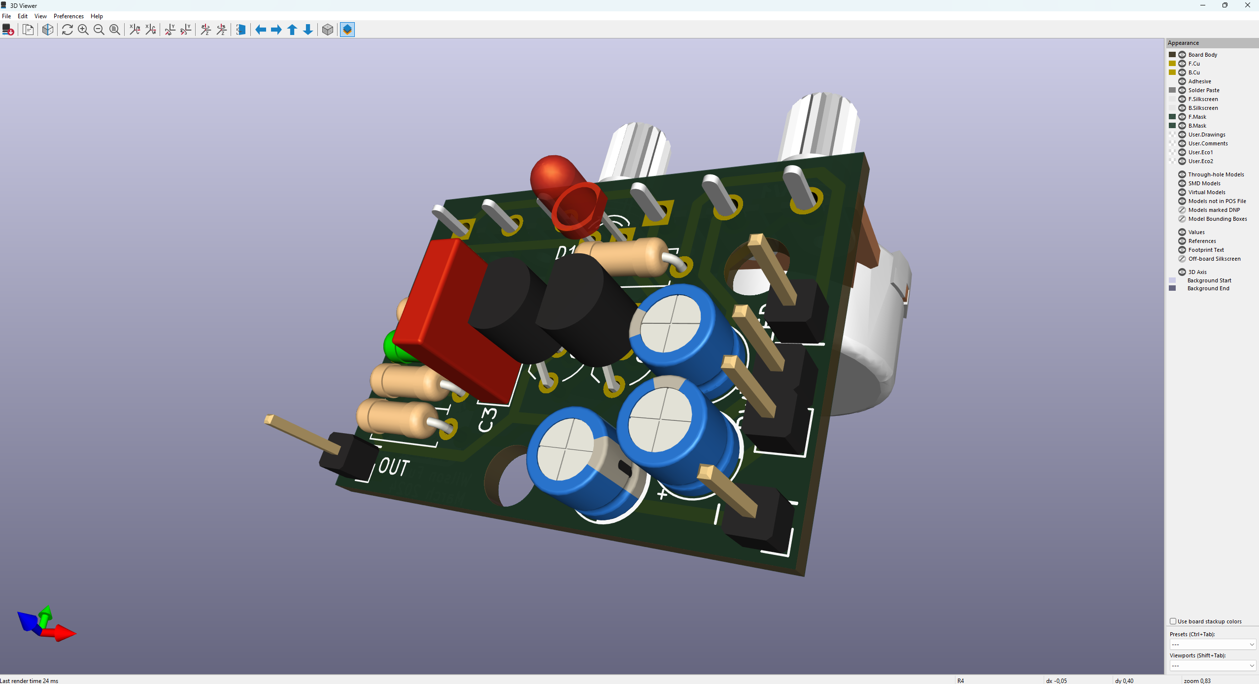
5. 3D preview of the PCB
-
When the PCB is ready, view it in KiCad’s 3D Viewer: 3D PCB Viewer Features | KiCad EDA
-
If component symbols have 3D models assigned, they will appear in the preview
-
Rotate the model, hide layers, and adjust the view
6. Exporting the 3D model to STEP format
-
In KiCad, export the finished PCB’s 3D model to STEP format
-
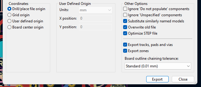
The function is located in the PCB editor under Export → STEP
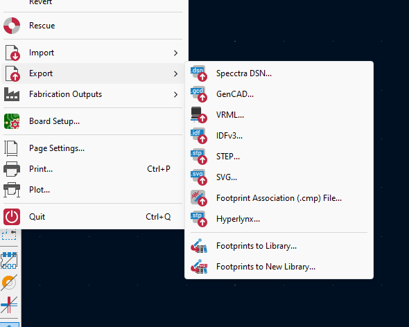
-
STEP export settings allow you to choose the level of detail in the model
7. Importing the 3D model into Vertex G4
-
In Vertex G4, open the model via File → Open File
-
The example PCB with components appears as an assembly
-
All components can be edited, hidden, or removed as needed
Note: In the example, the LED component contains ACIS geometry errors, causing the main assembly to appear in red. Correct or remodel the LED geometry to remove the error.
In Vertex G4, you can design housing structures around the PCB.
Example: A sheet metal enclosure for a Raspberry Pi designed in G4, with holes, PCB mounting, and enclosure fastening planned.
Enclosure construction could also be designed for 3D printing or injection molding.